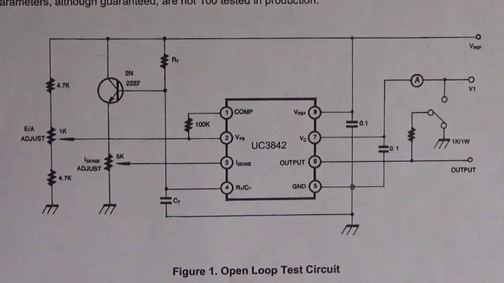
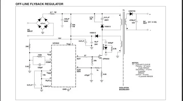
The UC3843 IC integrated circuit, also known as the UC3843, is a versatile and frequently used PWM (Pulse Width Modulation) controller developed for offline and DC-to-DC converter applications. This integrated circuit has various advantages that make it a popular choice for electronics enthusiasts and experts alike. In this post, we will look at the UC3843 IC circuit diagram in depth, including its pin arrangement, operating principles, and how it may be used in a variety of applications.
Overview of the UC3843 IC
The UC3843 IC is a high-performance fixed-frequency PWM controller with superior performance to typical PWM controllers. It is intended to provide more stability and control in power supply applications. Some of its important aspects are:
- High-performance current mode. PWM Control
- Low starting and operational current.
- High output current capability.
- Under-voltage lockout and hysteresis
- Features include over-temperature protection and programmable switching frequencies.
Key Specifications:
Before digging into the circuit schematic, it’s important to grasp the key specifications of the UC3843 IC:
- Operating voltage range: 7.6 to 30 volts
- Output Current: Up to 1 A
- Operating frequency: up to 500 kHz (programmable).
- Current Sense Threshold: 1V (Typical)
- Startup current: 0.5 mA (typical).
- Operating current: 12 mA (typical).
- Temperature range is -40°C to +85°C.
These parameters make the UC3843 IC appropriate for a wide range of applications, including basic DC-to-DC converters and more complex switch-mode power supplies (SMPS).
Pin Configuration
Understanding the UC3843 IC’s pin arrangement is critical for circuit design and implementation. The IC comes in an 8-pin package, with each pin having a specific function.
- Compensation (COMP): This pin controls frequency and stability.
- Voltage Feedback (VFB): This pin accepts feedback voltage from the output.
- Current Sense (CS): This pin monitors the current passing through the inductor.
- RT/CT: This pin controls the oscillator frequency.
- Ground (GND): The common ground pin.
- This pin sends a PWM signal to the gate of the power MOSFET.
- VCC is the supply voltage pin.
- Ref (REF): This pin supplies a reference voltage.
How to Make a Multimeter using an Android Mobile
Each of these pins is critical to the operation of the UC3843 integrated circuits, and understanding their functions is essential for constructing effective circuits.
3843 Integrated Circuit Diagram
The circuit schematic below shows how to use the UC3843 IC in a DC-to-DC converter application. This example shows how a basic buck converter lowers down the input voltage to a lower output value.
Components List
- UC3843 IC: The PWM controller.
- Power MOSFET: serves as the primary switching device.
- Inductor (L1): Stores energy and smoothes output current.
- Capacitors (C1, C2) filter the input and output voltages.
- Diode (D1): Provides a channel for the inductor current when the MOSFET is turned off.
- Resistors (R1, R2): Establish the feedback and compensation network.
Working Principle
The operation of the UC3843 IC in a buck converter circuit can be divided into various stages:
- Start-Up: When the input voltage is provided, the UC3843 IC initiates its startup procedure. The under-voltage lockout (UVLO) circuit ensures that the IC only operates when the supply voltage exceeds a specific threshold. This prevents the IC from malfunctioning owing to a low supply voltage.
- Oscillation: The RT/CT pin controls the oscillator frequency, which influences the switching frequency of the PWM signal. A resistor and capacitor attached to this pin control the oscillator’s timing, which is critical for determining the converter’s operating frequency.
- Feedback and Control: The feedback voltage from the output is sent into the VFB pin and compared to an internal reference voltage. The error amplifier modifies the PWM duty cycle to ensure a consistent output voltage. If the output voltage is too high, the duty cycle is decreased; if it is too low, the duty cycle is increased.
- Current Sensing: The CS pin detects the current passing through the inductor. If the current reaches a predetermined limit, the IC lowers the duty cycle to avoid overcurrent problems. This current limiting mechanism prevents circuit components from harm caused by excessive current.
- PWM Output: The OUT pin sends the PWM signal to the gate of the power MOSFET, which controls the MOSFET’s on and off states. This regulates the amount of energy transmitted to the output. When the MOSFET turns on, energy is stored in the inductor. When it is turned off, the energy is transmitted to the load via the diode.
Detailed Circuit Diagram Explanation
To have a better understanding, let’s deconstruct a typical application circuit that employs the UC3843 IC in greater detail:

Power Supply
The VCC pin provides electricity to the UC3843 integrated circuit. This pin is connected to a capacitor (C1), which filters the supply voltage and provides the IC with a consistent working voltage. The voltage range for VCC is commonly 7.6V to 30V, and a regulated supply is required for stable functioning.
Oscillator Timing Network
The oscillator frequency is set by connecting the RT/CT pin to a resistor (R1) and a capacitor (C2). The values of R1 and C2 control the frequency of the PWM signal, which is critical to the converter’s functionality. The average operating frequency range is up to 500kHz.
Feedback Network
The VFB pin is connected to a voltage divider network made up of resistors (R3 and R4) from the output voltage. This network reduces the output voltage to a level that is comparable to the internal reference voltage. The error amplifier within the IC adjusts the PWM duty cycle based on the difference between the feedback and reference voltages.
Current Sensing Network
The CS pin is connected to a current measuring resistor (R5) that is in series with the power MOSFET. This resistor monitors the current passing through the inductor. If the current exceeds a predetermined threshold, the IC lowers the duty cycle to avoid overcurrent problems. This function is crucial for protecting circuit components from damage caused by excessive current.
Compensation Network
The COMP pin is connected to a compensation network made up of a resistor (R6) and a capacitor (C3). This network provides frequency correction and stability to the control loop. Proper compensation ensures that the converter runs smoothly and responds appropriately to variations in load or input voltage.
Output Stage
The OUT pin sends the PWM signal to the gate of the power MOSFET. This signal regulates the switching of the MOSFET, which modulates the energy transmitted to the output. A gate resistor (R7) is commonly used to manage the MOSFET’s switching speed and reduce electromagnetic interference (EMI).
Inductors and diodes
When the MOSFET is turned on, the inductor (L1) stores energy, and when it is turned off, it releases it. The diode (D1) allows the inductor current to flow when the MOSFET is turned off. This configuration ensures that the inductor’s stored energy is efficiently delivered to the load.
Practical applications
The UC3843 integrated circuit is widely employed in a variety of applications because of its adaptability and performance. Here are a few practical examples:

Switch Mode Power Supplies (SMPS)
The UC3843 IC is widely used in switch-mode power supply to enable efficient and steady power conversion. Whether it’s a basic buck converter, a boost converter, or a more complex flyback converter, the UC3843 IC provides the flexibility and control required for effective power management.
DC-to-DC converters
DC-to-DC converters convert one DC voltage level to another. The UC3843 IC is perfect for creating efficient and dependable DC-to-DC converters, whether they step down (buck converter) or up (boost converter) the input voltage.
Battery Chargers
Battery chargers must precisely control the charging current and voltage to provide safe and efficient charging. The UC3843 IC includes the characteristics required to create intelligent battery chargers that can handle a variety of battery chemistries and charging patterns.
LED drivers
LED drivers require constant current management to maintain consistent brightness and LED lifetime. The UC3843 IC can be used to create efficient LED drivers that maintain constant current management and safeguard the LEDs from overcurrent circumstances.
Motor Control Systems
The UC3843 IC can also be utilized in motor control systems to provide fine control over motor speed and torque. The UC3843 IC achieves smooth and efficient motor running by controlling the PWM signal sent to the motor.
Design Considerations
When constructing circuits with the UC3843 IC, several critical issues should be kept in mind:
Component Selection
Choosing the correct components is critical to the circuit’s performance and reliability. Make sure that the power MOSFET, inductor, capacitors, and diodes are qualified for the intended operating conditions. Pay close attention to factors like current rating, voltage rating, and switching frequency.
Thermal Management
Heat dissipation is an important part of power electronics design. To avoid overheating, ensure that all components, particularly the power MOSFET and inductor, are appropriately cooled. Use heat sinks and suitable PCB layout strategies to improve thermal management.
PCB Layout
Proper PCB layout is crucial for limiting electromagnetic interference (EMI) and guaranteeing stable operation. Shorten high-current pathways and minimize loop areas to reduce EMI. Ground planes and decoupling capacitors can increase noise immunity.
Frequency Compensation
Proper frequency compensation is required to guarantee that the control loop runs smoothly. Use the recommended compensation network parameters and test the circuit under different load conditions to ensure stability.
Protection Features
Implement protective features such as overcurrent, overvoltage, and thermal shutdown to improve the circuit’s reliability and safety. The UC3843 IC includes built-in protection mechanisms, although additional external protection may be required for some applications.
Conclusion
The UC3843 integrated circuit is a powerful and adaptable PWM controller that is used extensively in modern power electronics systems. Understanding its circuit diagram and how it works will help you create efficient and dependable power supply solutions. Whether you’re working on a basic buck converter or a sophisticated switch-mode power supply, the UC3843 IC provides the flexibility and performance you need.
Mastering the UC3843 IC will improve your ability to build and troubleshoot power electronics circuits, allowing you to become a more proficient and experienced electronics engineer. The UC3843 integrated circuit is a must-have instrument in the field of power electronics, thanks to its versatile applications and sturdy features.


